|
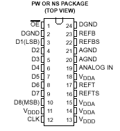
The new ADC module uses the TLC5540 high-speed, 8-bit "analog to digital" converter (ADC) that converts at sampling rates up to 40 megasamples per second (MSPS).
This ADC is a CMOS "semiflash" converter which uses pipelined dynamic conversion to achieve its high performance. The functional diagram below shows the pipeline architecture which results in a 4 sample delay between analogue data capture and digital data conversion. 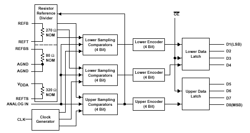
Because the sample is held as a charge, conversion accurracy depends on the sampling rate. That is, this chip prefers a fast clock, but not too fast as the 40 MHz option explains. The design also allows a much shorter aperture time which translates to a higher input capture bandwidth; very useful when sub-sampling. This compares with the original MC10319 ADC, which being a single stage bipolar "flash" converter means minimal propagation delay, but which is not capable of achieving such high input bandwidth data capture. |
Copyright © 2023 BitScope Designs