|
The ADC5540 module is designed to function similarly to the original MC10319 chip.
Schematic Diagram
You will notice from the schematic that there are a couple of extra components to set the VIN span and clip overvoltage inputs.
- R1 and R2 generate Vm and allow trimming of Input SPAN to exactly 2.0V. Vm is used to calibrate the ADC range to the middle of the input voltage.
- D2 diode clamps the input signal from going negative.
- D1 moves the ADC range up from GND (0.4V) to improve linearity for signals near 00h.
- R3 dampens the CLK signal to impove performance at high frequencies.
- C1-C6 decouple supplies to ground minimising noise.
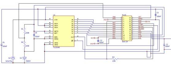
ADC 5540 module schematic (click here for PDF version).
PCB Layout
Key to the performance of this high speed converter is the PCB design...
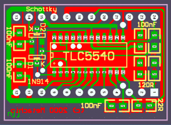
ADC 5540 module layout (enlarged x 2.5)
|
We have employed low noise surface mount technology with all the SMD components placed on the underside of the PCB.
This helps shield the sensitive circuit from noise by placing the active components "upside down" so they are located between the ADC module's ground plane and the BitScope PCB.
Note the location of the ground plane which is as large as practical and arranged to shield critical signals.
|
Signal Clipping
Sometimes the signal applied to BitScope may cause a signal in excess of 2Vpp at the ADC.
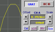
Clipping shows limit of ADC span
|
The input chain has been designed to ensure that the ADC will clip the signal. The positive clipping is handled by the ADC since the OP AMP driver runs from +/-5V, Vin at the ADC must always be less than +5. For negative clipping a schottky diode is used on the ADC5540 module so Vin never exceeds -0.4V, which is within spec for the ADC chip.
|
With previous ADC modules BitScope included a pair of back to back diodes for signal clipping. These diodes are not required with the ADC5540 module.
|


