|
After the range selector the analog signal is buffered and amplified by U16. 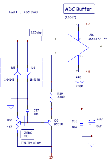
This stage has a gain of 1.667 which takes an input clamped at ±0.6v and outputs a ±1.0v signal. The output offset is set by emitter follower Q5 and RV1. Adjusting RV1 will shift the signal span to match the input of the A/D module being used. For example: (1) The Motorola ADC has a 2V span centered at 1V. (2) The AD9057 has a 1V span centered at 2.5V (3) The TI TLC5540 has a 2V span centered at 1.62V Diode clamps on the input to U16 ensure that the input to the ADC never exceeds 2V p-p. Some ADC chips do not tolerate overvoltage on the input. Current limiting resistors R38, R29 ensure that the mighty MAXIM drivers do not exceed the current limits of the Range Select multiplexer. The ADC Buffer provides a low impedance drive for the ADC, which may be a few hundred ohms and 30 pF or so. Note that C27 takes off the AC component of the input to the ADC for edge counting in Spock. RV2 is connected to pin 24 of the ADC to adjust the span. This allows the span to be calibrated if possible for the particular ADC in use. |
Copyright © 2023 BitScope Designs


