|
BitScope's modular A/D interface allows the use of more than one type of A/D convertor. 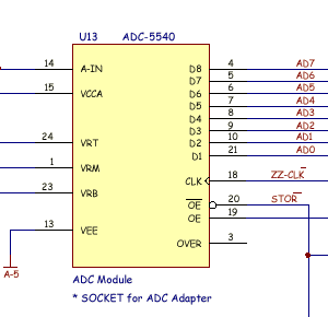
The interface itself is simple. The data bus drives the Analog SRAM, Spock and MUX. The sample clock is the same zz-clk used by Spock and !STORE drives the !OE pin. The "nominal" A/D convertor for BitScope is the now obsolete Motorola MC10319 "Flash Convertor" which used a comparator tree and gray scale decoder allowing it to be clocked from 25MHz down to DC. When BitScope was designed, this A/D convertor was already "on its way out", so why design in an outdated chip ? Because it's the perfect footprint for a replaceable A/D Module ! The MC10319 was available in a 24pin 600mil package. It used all the analog and digital power supplies, data bus, and control signals as required by any A/D convertor. Rather than design a new PCB for every different ADC chip on the market (which are all surface mount now anyway) it seemed a better bet to design for the Motorola part, then make a 24pin 600mil "carrier" PCB for each new Flash ADC of interest. If you examine the spec sheets on a many A/D convertors, you will see they work in much the same way. The only real difference is the input offset and span details. The module scheme adopted in BitScope is quite flexible. It is even conceivable that a 16 bit ADC module could be devised that outputs odd/even byte pairs. |
Copyright © 2023 BitScope Designs


